INTERFACE LAYOUT – top side
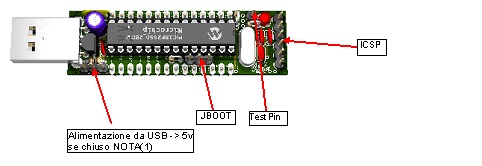
The top side of the board is shown in the next picture:
You can see three Jumpers:
- Power supply selection
- Boot loader selection
- ICSP programming interface
Last, you can find the Test Input PIN, this PIN can be used to drive the RED LED on the board.
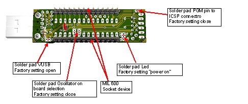
INTERFACE LAYOUT – bottom side
In the following picture you can see all optional solder pads you can use depending of the PIC you use.
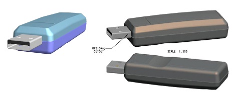
USB DONGLE-BOX LAYOUT
The dongle-box is shown in the following picture
APPLICATION SCHEME
This is the application scheme for Piccoletta
Click on the picture to enlarge..
BILL OF MATERIALS
Here you are the bill of materials
| Componenets | Value | Description |
| C1 | 470n | Metallized PE Film Capacitor C050-025X075 |
| C2, C6 | 0,1uF | Metallized PE Film CApacitor C025-024X044 |
| C7 | 0,1uF | Metallized PE Film CApacitor C025-024X044 (Not mounted) |
| C3 | 10uF 18V | Capacitor Electrolitic Radial (5x11x2,5) CPOL-EUE2-5 |
| C4, C5 | 18pf | Metallized PE Film CApacitor C050-024X044 |
| R2, R5 | 10K 1% | Metal film resistor (0204) 0,4 Watt |
| R4 | 10K 1% | Metal film resistor (0204) 0,4 Watt |
| R3 | 3,3K 1% | Metal film resistor (0204) 0,4 Watt |
| R1 | 10 Ohm 1% | Metal film resistor (0204) 0,4 Watt |
| IC1 | PIC18F2550_28DIP | |
| L1 | Led 3mm RED | 15 mcd 40° |
| J1 |
Double pin header instead of triple pin header. Pin # 1 is not used. |
pin 2–3 open: power supply from expansion board.
|
| J-boot | Triple pin header | Boot pin header Pin 2 – 3 connected -> A VCC is applied on the pin of PIC Pin 1 – 2 connected -> GND on the pin of PIC |
| ICSP | 6 pin header | ICSP PIC programming connector pin Pin 1 Vpp « MCLR pin pic Pin 2 Vcc « Pin 3 Gnd « Pin 4 PGD « PGD pin pic Pin 5 PGC « PGC pin pic Pin 6 PGM « PGM pin pic |
| T | 1 pin header | Test pin led |
| T1 | 3 solder pad |
Solder pad jumper con fori per ponticello riporta le seguenti selezioni vedi figura layout circuito Top Side Pin 1 – 2 connected -> RED LED on with power supply |
| S1 | 2 solder pad | Used on the pin VUSB for the 3.3 V configuration. S1 « closed Normal power supply 5V S1 « open (factory setting) |
| S2, S3 | 2 solder pad |
Select the oscillator on the PCB S2, S3 « open the oscillator on the expansion board is selected |
| S4 | 2 solder pad | Used to disconnect the PGM pin from the ICSP connector S4 « closed (factory setting) Normal power supply (5V), S4 « open |
| Q1 | 8Mhz oscillator | HC49U-V |
| IC2 | MCP1700 | Microchip LDO regulator 250mA (non mounted) |
| USB connector | USB-A-H |
If you want to give us support or if you want the assembled and tested board, you can go to ebay at the following adress:
http://shop.ebay.it/giovannitto/m.html?_dmd=1&_ipg=50&_sop=12&_rdc=1
Gg1


Do you have a source for the dongle-style plastic case?
Keep up the good work…
Marco
P.S.: do you proofread your writings? The sentence "Here you are the bill of materials" in italian would translate "qui tu sei l'elenco dei materiali". Sounds funny, isn't it ?
For now we don't have a source for the dongle-style plastic case. we are using old some old boxes found in the cellar.
anyway I'm reading "il Sansoni Inglese"
Ecco: (seguito da pronomi personali) here, there (seguiti da soggetto e verbo essere): eccomi! (o eccomi qua!) here I am!; eccoti! here you are, there you are;eccolo! here he is, there he is; (riferito a cosa) here it is, there it is; eccola! (oeccola qua!) here she is, there she is; eccoLe il denaro here is your money; eccoci!here we are; eccovi! here you are, there you are; eccoli qua! here they are; vuoi il mio consiglio? eccolo do you want my advice? this is it (o here it is); eccoti nuovamente ubriaco there you are, drunk again; eccotelo! here you are, there you go; eccone uno here's one; eccone alcuni here are some; eccolo che arriva here he comes.
So it sounds good… and The sentence "Here you are the bill of materials" in italian is "Ecco a voi l'elenco dei materiali".
😉