How to use the MCP79410 Real Time Clock
In this article I'm going to show you how to use the MCP 79410 we have mounted on our boards.
- Temperature sensor and real time clock for Arduino
- A PIC 12f1840 developer board with mcp79410 RTC and tcn75 temperature sensor.
The MCP79410 is a Real Time Clock (RTC) chip that uses a digital compensation of the time to realize an accurate clock/calendar. It has a programmable output line (it is possible to program up to two alarms), it can be backupped by an external battery (there is an ad hoc circuit), it has a small non volatile memory to store data and a small backupped SRAM.
The MCP79410 communicates over an I2C™ bus.
The clock/calendar automatically reguates itself with months up to 30 days. The clock works fine with the 24 hours format or with the 12 hours foramt with an AM/PM indicator.
It provides a programmable output pin that can be used as a configurable alarm or it can be used as a frequency generator working at 32,768, 8,192 e 4,096 kHz e 1 Hz.
The last frequency cannot be used when the power supply comes from the backup battery.
It also provides an EEPROM, a backupped SRAM, 64 bits of non volatile space that can be used for a unique ID or for a MAC Address.
The devices is completely accessible trough the I2C™ serial port and it needs a Vcc in the [1,8..5,5]V range
The most important characteristics of this chip are the following:
- Automatically manages days, months, years etc etc
- Automatically manages hours (12 AM/PM format or 24 hours format.
- Automatically manages the days of a week (first, second,….)
- SRAM 64 bytes long, it can be powered by a backup battery
- Two programmable alarms.
- One Open/Drain output used to receive a clk signal (32768hz, 8192hz, 4096hz e 1hz) or to generate an alarm.
- 1 Kbit EEPROM (8 bytes pages)
- another 64 bits EEPROM normally used as unique id.
- i2c bus to communicate with the world (100Khz.400Khz)
- It can be powered with voltages from 1,8 to 5 volts (i2C).
- RTCC working is granted with voltages dont to 1,3 volts (timekeeping and SRAM backup)
- It can be calibrated to achieve precision of 1ppm
- It automatically switches between normal power supply and backup power supply.
- While using the backup battery it cannot be accessed trhough the i2c bus
- Working temperature [-45, +80]°C
On the i2c bus, the device will be addressed using the following addresses :
| Address | Desription |
| 10101110 | Write on EEPROM and unique ID |
| 10101111 | Read from EEPROM and unique ID |
| 11011110 | Write on SRAM and Registers |
| 11011111 | Read from SRAM and Registers |
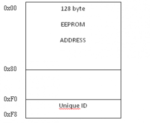
The address space for the EEPROM includes the unique ID
While the address space for the SRAM and the device registers is as follows:
To have more details please refer to Microchip documentation (DS22266C)
Some registers of the RTCC 79410 contain values in BCD notation so we'll need of to convertion functions:
// Converts a decimal number to a BCD number
char dec2bcd(char num)
{
  return ((num/10 * 16) + (num % 10));
}

// Converts a BCD number to a decimal number
char bcd2dec(char num)
{
  return ((num/16 * 10) + (num % 16));
}
The RTCC registers
At address 0x00h you'll find seconds and tens of seconds (BCD notation) the ST bit is used to start/stop (1/0) the clock
At address 0x01h you'll find minutes and tens of minutes (BCD notation)
At address 0x02h you'll find hours and tens of hours (BCD notation). The AM/PM bit and the 10/hours bit select the AM/PM or 24h format.
At address 0x03h you'll find the day (BCD notation [1, 7])
At address 0x04h you'll find date and date in tens in BCD notation ([01, 31]).
At address 0x05h you'll find the month and the month in tens in BCD notation. The fifth bit is readonly and if it's value is 1 the year is a bisextile year.
At address 0x06h you'll find the year and the year in tens in BCD notation. ([00, 99])
At address 0x07h you'll find the Control Register.
BIT 7: It sets the logical level of the MFP when the MFP pin is not used as square wave output.
BIT 6: It is the SQWE bit. Setting this bit, the crystal divisor for the signal generation bit is enabled.
BIT 5,4: They set the activated alarms:
– 00 – None
– 01 – Alarm 0 activated
– 10 – Alarm 1 activated
– 11 – Both alarms activated
BIT 3: it enables EXT0SC. When its values is 1 the RTCC can be driven by a 32.768 Khz signal, avoid the need of an external crystal.
BIT 2-0: They set the internal divisor for the 32.768 Khz oscillator used to drive the MFP pin. The duty cycle of the square wave is 50%. The following frequencies can be selected:
– 000 – 1 Hz
– 001 – 4.096 kHz
– 010 – 8.192 kHz
– 011 – 32.768 kHz
– 1xx enables the calibration function. The calibration function generate an output wave on the MFP pin if the SQWE has been previously set (64hz nominal).
At address 0x08h you'll find the calibration register, its value is used added or removed from the RTCC counter (each minute). The MSB bit select the addistion or the subtraction. The remaining 7 bits give to the user the capability to add or subtract up to 254 clock cycles a minute.
At address 0x09h you'll find the Unlock Register. To wrote on the unique ID area, a specific sequence must be executed.
At addresses 0x0Ah-0x0Fh and 0x11h-0x16h you'll find the registers for the two alarms (Alarm0 and Alarm1)
At addresses 0x10h and 0x17h you'll find two reserved registers. (you should not use them)
For now we'll ignore all others registers.
Speaking to the device
To speak to the device we will use the functions defined for the Pic 12f1840 in this post.
| void i2c_start(void) | sends the start bit |
| void i2c_restart(void) | sends the restart bit |
| void i2c_stop(void) | sends the stop bit |
| void i2c_ack(void) | sends ACK |
| void i2c_nack(void) | sends NACK |
| void i2c_wr(unsigned char i2c_data) | |
| unsigned char i2c_rd(void) |
SRAM writing sequence
void sramWriteSequence()
{
  gucI2CError = 0;       // zero the I2C error
  i2c_start();           // start I2C communication
  i2c_wr(0b11011110 | 0);// write DEVICE ADDR for SRAM WRITES
  i2c_wr(rtcc_reg);      // write the register's rtcc_reg
  i2c_wr(time_var);      // write a byte (variable time_var)  in the register
  i2c_stop();            // stop I2C communication
}
EEPROM writing sequence
void eepromWriteSequence()
{
  gucI2CError = 0;        // zero the I2C error
  i2c_start();            // start I2C communication
  i2c_wr(0b10101110 | 0); // write DEVICE ADDR for SRAM WRITES
  i2c_wr(rtcc_reg);       // write the register's ADDRESS
  i2c_wr(time_var);       // write byte variable in the register
  i2c_stop();             // stop I2C communication
}
EEPROM reading sequence
void eepromReadSequence()
{
  gucI2CError = 0;  // zero the I2C error
  i2c_start();// start I2C communication
  i2c_wr(b10101110 | 0);// write DEVICE ADDR for RTCC WRITES
  i2c_wr(rtcc_reg);// write the register ADDRESS
  i2c_restart();// RESTART for READS
  i2c_wr(b10101110 | 1);// send the DEVICE ADDRESS for RTCC READS.
  rtcc_buf = i2c_rd();// read register (stored in 'rtcc_buf')
  i2c_nack();// NOACK from MASTER (last read byte)
  i2c_stop();// stop I2C communication
}
Gg1


